HP Articles Forum
[Return to the Index ]
[ Previous | Next ]
Enhance your HP-97 -- Add a Clock and More
Posted by Katie Wasserman on 1 Sept 2009, 6:53 p.m.
The HP-97 and HP-97S are identical except for the addition of the I/O pod on the 97S. This project demonstrates how it is possible to achieve some of the functionality of the 97S (including the pod) on a plain HP-97. In particular, it demonstrates how input can be feed to a 97 in the same way that the 97S pod does, only more so....
disclaimer: The control lines from an HP-97S to it's pod are only partially documented in the HP-97 service manual and the HP-97S Operation Guide. So, much of the following is from a bit of reverse engineering and therefore subject to inaccuracies.
On the HP-97S and newer HP-97 calculators all the control lines needed for the pod interface are conveniently brought to a 16 pin DIP socket location on the main logic board, but they exist on the earlier model HP-97 calculators as well, they are just not so conveniently accessed.
These are all the control lines along with their pin assignments on the DIP header:
 Control Line     Header Pin #
--------------    ------------
    GND              1
    n/c              2
    phi-1            3
    phi-2            4
    RCD              5
    KBA              6
    KBC              7
    KBD              8
    +V               9
    +V              10
    STR             11
    KBE             12
    DATA            13
    SYNC            14
    IS/IA           15
    GND             16
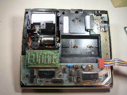
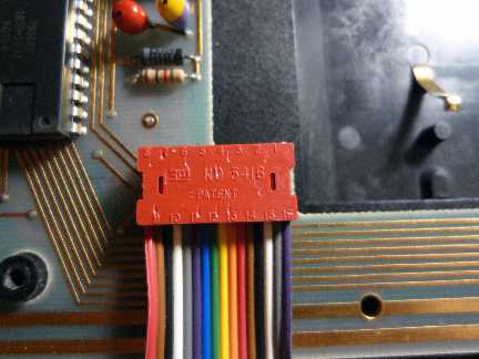
Here's a picture of the main board in the 97S (and newer 97). Note the ribbon cable that has replaced the standard cable that attaches to the pod and the closeup show the pin numbers on the IDC DIP header
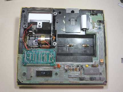
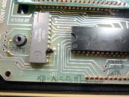
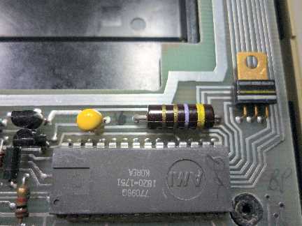
Here's a picture of the main board in an older 97 and a closeup show the locations of the needed control lines for this project.
Inspection of the Keyboard PCA Schematic Diagram in the HP-97 service manual shows that a 1-of-14 counter/decoder chip (labeled as the cathode driver since it servers that purpose too) is used to scan the rows of the keyboard matrix. These 14 rows times the 4 columns (KBA, KBC, KBD, KBE) account for all 64 keys on the HP-97. The 14 outputs from the cathode driver chip are normally high and only go low when the row is being scanned. If a key on that row is pressed it will complete the circuit to one of the 4 column lines. So, pulling a column line low at the moment when the needed row is selected is equivalent to pressing the corresponding key. In this way, keyboard input can be simulated by an external circuit. The cathode driver chip is clocked by the rising edge of STR (strobe?) line and reset by the falling edge of RCD (reset cathode driver?) line. Knowing this it is straightforward to program a microcontroller chip to simulate key presses using these 6 control lines.
The 97S pod uses all of the lines coming out of the DIP header, why? The DATA, IS/IA (serial address), clock lines (phi-1 and phi-2) and SYNC lines are needed to capture the commands that the HP-97S is executing. Actually, the 97S only looks for 8 commands: Set Flag 0, Clear Flag 0 and the same for flags 1, 2 and 3. It uses these commands to set/clear 4 output lines on it's 50-pin connector and to indicate that the calculator is ready for input from the user. This project makes no attempt to decode the address and data lines on the 97 and therefore has no flag output lines. However there is a simple way that the calculator can indicate that it is ready for input.
As it turns out, the DATA line has nearly continuous activity on it except when the number the calculator is displaying has a value of zero in the X register and is awaiting keyboard input. In this state, there are no signals on the DATA line (but there is a lot of noise for some reason -- a Schmitt trigger input can be used to overcome this problem). Thus a program running on the 97 can simply clear the X register and execute a R/S command to indicate to an external microcontroller-based interface that it's ready for input. The external processor can then key in the numeric input followed by a R/S command to resume the program.
This project makes use of all of the above findings to enhance the basic HP97. It's composed of a simple microcontroller, a Parallax SX28 with just 2K of ROM and 136 bytes of RAM, along with a DS1302 real time clock chip that is used for timekeeping and non-volatile memory. The SX not only simulates key presses on the 97 it also reads the keystrokes that the user presses on the 97. This is how the user tells the external microcontroller what functions to preform (e.g., set the time on the clock or generate a random number). Taken together -- 97 keyboard used to control the SX, SX used to control the 97 -- some useful enhancements can be implemented.
Since all the keys on the 97 do something, there needs to be a way to talk to the SX without the 97 doing anything, at least anything critical. There are several commands that don't make much sense in non-programming mode, for example x<0? and DEL, these are used with the additional precaution of a double press of the 'f' key to prefix them.
Here's the complete list of commands to talk to the SX microcontroller that are implemented in this project:
f,f,7 -- start the continuously updating real time clock display (show: HH.MM SS)f,f,1 -- stop the clock display
f,f,4 -- start the by request (CLX, R/S) updating real time clock entry (entry will be: HH.MMSS, R/S)
f,f,+ -- set the clock. The display is cleared and the user needs to enter HH.MMSS (24-hour format -- enter leading zeros)
f,f,- -- set the clock to 12 hour display format
f,f,x -- set the clock to 24 hour display format
f,f,8 -- set the number of seconds between display updates when the continuous clock is running. The display is cleared and the user needs to enter the number of seconds SS (enter a leading zero if needed).
f,f,RND -- generate a random number from 0-1 in the X register.
f,f,DSP -- show the scanning col.row of each subsequent keystroke. This is useful for making further enhancements and saves time rather than trying to read this from the service manual.
f,f,5 -- macro record. This will capture the next sequence of keystrokes (up to 26) and save them in non-volatile memory. To stop recording turn off the calculator. When the calculator is switched back on the keystrokes will be replayed. This is useful for storing often used constants in particular registers, setting default decimal places, etc.
note: Execution of each command occurs when the key pressed is released. When the clock is displayed and changing rapidly it is necessary to press and hold 'f' and command keys for 1 second or so to overcome any interference from the microcontroller trying to update the display.
The electronics of this project are simple, just the SX28, DS1302, a 32768Hz clock crystal and a small lithium battery for the DS1302. All the work is done in the firmware. The SX28 microcontroller source for this project is written in a BASIC-like language called SX/B that Parallax makes freely available. It's an extremely simple, compiled language with some built-in speciality commands that came form Parallax's Basic Stamp. The compiler is so simple that only a single arithmetic operation can be done in an assignment statement. If you look through the code you'll see all sorts of unreasonable things that are there just to fit this amount of stuff into 2K of ROM and to deal with the complier's limitations. I'm certainly no expert SX/B programmer so I'm sure there's room for improvement. It's not a pretty language nor a pretty program but hopefully the code is readable enough.
I choose the SX chip and SX/B just because I had them around and had a bit of experience using them. A better choice might have been to use a microcontroller with a built-in RTC, more memory, etc.
The schematic is simple enough for character drawing:
          Parallax SX28 (DIP)
         ---------------------       10K
        | 1-RTCC       MCLR-28|-----\/\/\---- Vb
  Vb ---| 2-Vdd        OSC1-27|---> to SX-key header pin 1       DS1302 RTC (DIP)
        | 3-n/c        OSC2-26|---> to SX-key header pin 2      -------------
 GND ---| 4-Vss         RC7-25|--------------------------------|5-CE    GND-4|--GND
        | 5-n/c         RC6-24|--------------------------------|6-I/O  XTAL-3|-------|//|--|  32768Hz Xtal
        | 6-RA0         RC5-23|--------------------------------|7-SCLK XTAL-2|-------------|  (6pf)
        | 7-RA1         RC4-22|                              +-|8-V2     V1-1|--Vb
        | 8-RA2         RC3-21|                              |  -------------
        | 9-RA3         RC2-20|                              |
 KBA ---|10-RB0         RC1-19|                             ----                 Vb
 KBC ---|11-RB1         RC0-18|                              --  3V lithium      |
 KBD ---|12-RB2         RB7-17|                             ----  CR1225         |
 KBE ---|13-RB3         RB6-16|--- DATA                      --                 --- .1uf bypass
 STR ---|14-RB4         RB5-15|--- RCD                       |                  ---  capacitor
         ---------------------                               |                   |
                                                             |                   |
                                                            GND                 GND
      SX-Key in-circuit programming header
        ---
       | 1 | -- OSC1                                Vb - is the calculator battery voltage
       | 2 | -- OSC2                                     (goes through ON-OFF switch)
       | 3 | -- Vdd                                GND - is common to calculator
       | 4 | -- Vss
        ---
Here's a picture of the prototype and how it fits inside the 97 case. There's a perfect space for it just above battery compartment and it mounts directly onto the exposed ends of the screws holding the security tab in place.

I've made a little video demonstrating the features. You'll see that this is a 97S but it had no pod so it's the same as a regular 97 only with the convenience of a 16 pin DIP header to access the needed control lines -- the missing pod was the impetus for this project.
[update: May 10, 2010] Etienne Victoria was successful in building this project and installing it in an HP-97 with the old style main circuit board. Pictures are here.
Much more can be done this, particularly if a different microcontroller with more memory is used. It would be easy to add a serial connection between a PC and the SX and use the PC to download programs into the 97. Digital and analog input from sensors can be feed via the SX to the 97. Many more commands can be added to the 97 using the 'f-f' prefix. The keystroke macro facility can be easily expanded to do all sorts of stuff, etc..
Edited: 11 Oct 2014, 2:02 p.m.