 The Museum of HP Calculators
HP Articles Forum
[Return to the Index ]
[ Previous | Next ]
HP-80 History, Design and Interesting Facts
Posted by Max Stone on 24 Oct 2013, 4:14 p.m.
The World’s First Businessman’s Pocket Calculator
Introduction
Hewlett-Packard redefined portable computing with the launch of the HP-35 in 1972. This was the world’s first pocket calculator with transcendental functions (sin, log, etc.) and the first with RPN (Reverse Polish Notation). Overnight, the slide rule was dead.
A month after the launch of the HP-35, Bill Hewlett had breakfast with 200 securities analysts in New York. HP had placed HP-35s at each breakfast table and Bill noticed that “…although they were familiar with electronics, it was evident that such key designations as sin, cos, log and ex were more a barrier to an understanding of the calculator's function than a help…Right there and then it became evident that what was needed was a pocket-sized calculator designed specifically for the business community…”
Bill realized that there was a gap between the language of the financial user and their development engineers, so he put Bill Crowley from their corporate finance department together with France Rode, from HP Labs, who was an expert in programming and assigned the project leader of the HP-80 development team. The two visited a number of potential business users and from their discussions identified a basic set of financial problems that were eventually incorporated into the HP-80. HP had to develop many new financial algorithms to deal with the key-entry logic, design architecture and limited memory of the device.
Head of R&D and instrumental in the development of the HP-35, Barney Oliver helped arrange the keyboard to allow logical entry of financial problems. With over 30 financial functions, it was necessary to provide shifted functions on several keys, so the HP-80 became HP’s first calculator to feature the now famous unlabeled gold prefix key that continues on HP calculators to this day.

In four short months, HP had locked-down the details of the Model 80 which was essentially a modified HP-35 sharing the same architecture, but now with a total of seven ROMs (up from three) for the microcode and the higher-level functional implementations. The seven ROMs were mounted on a hybrid circuit to form a single assembly, with each ROM containing 256 ten-bit words, giving a total ROM memory size of approximately 2Kb. (Image above shows the hybrid chip with the seven ROMs in a row. These are protected under a metal cover in production.)
By mid-December HP had started limited production. The HP-80 was unveiled to the world’s media on 16 January 1973 at 15 press conferences around the world. The price for the HP-80 at launch was $395 and was supplied in a protective case that held the calculator and accessories (leather case, AC adapter and manual).
Several versions of the HP-80 were released over its lifetime but these were mainly minor cosmetic variations with the exception of the final production version that used quad ROMs (two HP-45/55/70 style DIPs) rather than the seven ROM hybrid. Unlike the HP-35, the HP-80 had no significant bugs when it was first released. The HP-80 was discontinued in 1978, replaced by the HP38E introduced that same year. During its lifetime, the HP-80 witnessed the launch of the remaining ‘Classic’ series calculators, the second generation (“Woodstock”) and many of the third generation (“Spice”) calculators.
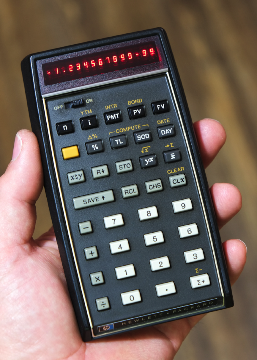
There are many HP-80s still in circulation, even after being discontinued 35 years ago. This document is a detailed (but not exhaustive) overview of the HP-80 including photographs from an example I recently acquired.
What’s in the Box?
The first HP-80’s were supplied in a vinyl-covered metal carry case with snap closure. The plastic liners have a type of felt coating with moulded pockets and cut-outs for storing the calculator and accessories securely.
The 78-page Owner’s Handbook is stored in the lid pocket and has a pocket in the inside back cover for the Service card and Addenda card. There is an Accessories brochure that lists optional accessories for the HP-35 and HP-80 including the security cradle, field case and battery holder (charger). There is also a 20-page spiral-bound Quick Reference Guide that fits inside a pocket of the separate leather case. The battery charger/AC Adapter is switchable between 110V and 220V and has the part number 82002A.
Later HP-80s were supplied with a plastic carry case and a synthetic leather calculator case. This example is also the early version of the HP-80 with only the words "Hewlett-Packard" on the bottom edge. Later versions added the model number "80". The OFF/ON wording next to the power switch was changed from printed text (as here) to raised molded letters in later versions.
Exploring the Design and Internals of the HP-80 Calculator
The serial number of this example is 1247A05774. While this suggests a production date of December 1972, HP’s early calculators used the first four digits to track version numbers indicating that this example was from the earliest product batch that started at the end of 1972. The opened calculator reveals a production date around January 1973.

Like all Classic series calculators, the HP-80 is quite easy to open. There are six screws holding the case together. Two are inside the battery compartment, two are below the bottom rubber feet and two are below the top edge of the rear label. Getting to the screws below the label requires that the label is carefully peeled back. The label is thin aluminium and it can be gently lifted and pulled back from a corner if the glue is released with some heat from a hairdryer. It’s nearly impossible to avoid some creasing of this label so you must accept some imperfections when pressing it back into place. The right screw is just below the ‘S’ of the word “INSTRUCTIONS” so only about one quarter of the label needs to be peeled back.
All the fasteners used in the HP-80 are zinc plated self-tapping steel screws and all had a fine white crystalline coating on the exposed head from 40 years of airborne contamination. The deposit easily rubs off but leaves the screw head a dull color.

The image above shows the calculator with the back removed. The two sets of 4 passive components on the far left are coils used in the inductive circuit to drive the LEDs. This is a different approach where the current driving the LEDs is limited by the time it takes to build up in the inductor, rather than through a resistor in conventional LED displays. This strobed inductive drive circuit is more efficient and was invented and patented by HP for use in calculators. In the worst case, display power consumption is about 110 milliwatts (thirteen 8’s and two minus signs). The LED display is covered later in more detail.
The connector for the AC adapter is between these coils. The red and black wires connect the battery connectors to the circuit board. There is a metal-sprung connector held in the back cover (not visible here) that acts as a switch when connecting the AC adapter by isolating the battery circuit from the calculator (to allow charging) when the connector is inserted. This is why the HP-80 won't tun on if the AC adaptor is plugged in but off at the wall socket. Although gold-plated, the metal-sprung connector can corrode with the result that the connection fails and the battery cannot power the calculator. This example had unreliable operation when on battery power as a result of corrosion at this location, with the gold-plating flaking off the metal.
The HP-80 does not have a single CPU but contains five MOS/LSI (metal-oxide-semiconductor, large-scale-integration) circuits made up of seven read-only-memories (ROMs), an arithmetic and register circuit (A&R), and a control and timing circuit (C&T). The logic design was done by HP and the circuits were developed and manufactured by two outside vendors. Three custom bipolar circuits were manufactured by HP's Santa Clara Division: a two-phase clock driver, an LED anode driver/clock generator, and an LED cathode driver. (The block diagram below was taken from HP’s 1972 patent document and shows these circuits).
The three MOS circuits are two-phase dynamic MOS/LSI circuits with low thresholds allowing compatibility with TTL bipolar circuits and allowing extremely low-power operation (less than 100 milliwatts for all three MOS circuits). They are organized to process 14 digit BCD (binary-coded decimal) words in a digit-serial, bit-serial manner. The maximum bit rate or clock frequency is 200 kHz, which gives a word time of 280 microseconds, permitting a floating point addition to be completed in 60 milliseconds, or about 17 a second. (A 3 GHz Pentium 4 can do about 3 billion additions per second!)
In total, the LSI P-channel MOS circuitry in the HP-80 has about 40 thousand transistors. This is a little more than what Intel squeezed into the original 8086 in 1976, but a tiny fraction of the 1 billion transistors Intel now have keeping close company in the Core i7 chip.

The HP-80 uses two printed circuit boards for all the circuits shown above. There is a larger board that carries the keyboard connectors, the LED display, drivers and power connectors. The smaller circuit board (shown below) carries all the MOS logic, clock driver, and the power supply components. This is the "heart" of the HP-80 and a masterpiece of 1970's electronics design.

The seven ROMs are under the metal cover in the center of the circuit board (1813-0024). The passive components and transistors make up a power on signal circuit and DC to DC converter for the three supply voltages the calculator needs. The large white chip is the Control and Timing circuit (1820-0849), the smaller white chip is the Arithmetic and Register circuit (1820-0848) and the black chip is the bipolar clock driver. The row of connectors at the top connect to the keyboard circuit board that is sandwiched between a plastic internal frame and the front half of the case, and secured by the 8 screws.
Once opened you can see that while the serial number indicates a December 1972 batch number, the ROM chip is dated January 1973. Production dates are difficult to determine accurately as HP used pre-printed aluminium serial labels that started with 1247A (or S) for the early batch runs in America and Singapore, until the following 5 digits were no longer sufficient. Accurately dating these earlier versions is only possible by taking the calculator apart.

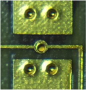
With the main circuit board removed, you can clearly see the connectors from the keyboard circuit board. Each is a tiny split spring that clips into its corresponding hole in the main processor board. There is no solder or latching mechanism and the main processor board is held in place by these connectors and two locating holes that match the two lower screw bosses.
The 8 screws holding the internal plastic frame also had surface corrosion, but like the external case screws, the white powder was easy to clean off. With these screws removed, the plastic frame and keyboard circuit board is released from the front half of the case. These assemblies are attached via wires leading from the battery and AC power connectors, visible at the right of the following image. The red leads terminate on the left and right pins of the AC adaptor connector, closed by the metal-sprung switch when the calculator runs on batteries. Clear insulation tape covers the soldered wires of the battery connector to prevent shorting on the circuit board.
The picture below shows the underside of the keyboard circuit board:

The picture below shows the keyboard circuit board, LEDs and related drivers. Also visible is the clear plastic layer that protects the internals from spills and dust that could otherwise enter the calculator around the keys. Also note the black rubber strip immediately below the LEDs. This strip prevents unsightly reflections off the pins below. I removed this strip for the remaining photographs.

The keyboard mechanical design of the HP-80 is identical to that designed for the HP-35, and patented by HP in 1971. HP calculators are famous for they keys, so they’re worth a closer inspection.

In their patent submission, HP describe the keyboard as a “reliable, low-profile, low cost keyboard with tactile feedback”. There are eight metal strips that run across the keyboard. Each of these strips has 4 or 5 small rectangular ‘humps’ less than 1mm high corresponding to each key, made by deforming (stretching) the metal in a shaped press. These strips are spot-welded to the circuit board and there are traces that run at right-angles spot welded to contacts that sit directly below the curved hump. Pressing the key makes contact allowing the calculator to identify the key by its grid location.

Mechanical bounce is less than one millisecond and the calculator contains a wait loop to prevent double entries. HP tested the design extensively and rate the design at over one million cycles. Critical to the success of this system and the overall feel of the key press, is the way the key has an “over-center” or “fall away” feel. When pressing the key, the operator must exceed 125 grams of pressure at which point the metal hump “breaks” through and electrical contact is made. The operator cannot prevent contact from happening once the break-point is reached, and when releasing the key, there is again a release-point when the operator cannot prevent the key from breaking contact. This patented design gives HP keyboards their distinctive feel and prevents missed or multiple entries. Even 40 years later, the keys have a crisp, accurate action because of this excellent design.
The final mechanical design feature worth mentioning is the way each key is hinged on the lower edge giving a rotational rocking motion when pressing the key. There is a clear plastic frame that fits below the entire keyboard and keeps each hinge located in the keyboard surround.

One of the biggest challenges in the HP-35 project was the design and implementation of the LED display. The HP-80 uses the identical LED design to the HP-35, as with the rest of Classic series of HP calculators.
The HP-80 uses three magnified five-digit clusters, saving both power and cost. Energy is stored in inductors and dumped into the light-emitting diodes using a pulse drive circuit. The LED display is made up of a 8 x 15 array of individual LED segments, 8 segments per digit (7 for the digit plus a decimal point) and 15 digits. Eight rows are scanned by the Anode driver (1820-1029) while the 15 columns are scanned by the 15 position shift register Cathode driver (1820-0854). The scanning operation moves from digit to digit in response to counter clock signals from the Anode driver.


The Anode driver circuit includes an LC circuit (resonant circuit) to set the scanning frequency of the display, made up of the black 150pF capacitor and 330 uH inductor to its left. The small resister above the inductor trims the reference voltage for detecting low power and turning on all the decimal points. The silver component to the right is a 2.2uF capacitor used to stabilize the power used by the LC circuit. The LC circuit generates a frequency of approximately 800 KHz, divided by 4 to 200 kHz by the flip-flop stage of the Anode driver circuit, and used to time the scanning of the display.
The solder points at the top of the board connect the 8 inductors used to drive the pulsed display circuit. Each inductor has a value of 130uH except the 68uf decimal point. The LED segments that make up each digit are pulsed individually, sweeping each digit sequentially and constantly refreshing the entire display at a speed too fast for the eye to see. (The blank delay when pressing a key is the display wait loop routine).
The display has 15 digits however the calculator’s word cycle is only 14 digits long. The extra character is the decimal point which is a special case as its position is generated by the Arithmetic and Register circuit or by the low voltage comparator in the Anode driver circuit that can trigger all decimal points to light up (indicating a low battery).
The three cluster of five LED digits each on the dual in-line package (DIP) in these images, with the moulded magnifying lens above each digit. Each DIP has 14 legs, connecting 8 anodes and 5 cathodes (one pin not connected internally). The common anodes across all three clusters are wired together while the 15 Cathodes are connected individually to the Cathode transistor switches.
The power switch contacts are visible below the Anode driver MOS chip. Even after 40 years, the grease on the board has not dried and the switch slides smoothly.

The first digit in the display is only used for the minus sign. The following 11 digits are used to display the mantissa and the decimal separator which occupies the space of an entire digit. The 13th digit displays the sign of the exponent and the last two digits display the two digit exponent:
-1.234567899-99
Later HP LED calculators had less characters in their displays. The Woodstock series had 12 digits however space was saved as the exponent shared space with the mantissa and the decimal point shared space with a displayed digit. The last LED-series calculators added a comma segment. HP launched their first LCD calculator, the HP-41C in 1979 and by 1983 HP had discontinued all their LED pocket calculators in favour of LCD models.
The Battery Rebuild
After 40 years the original NiCad battery pack was shot and was beginning to leak corrosive electrolyte. Fortunately the battery contacts of the Classic series are not at the ends of the battery but midway down so damage to the contacts can be avoided if the battery is not leaking too badly.
I split open the plastic carrier with a craft knife and replaced the three failed NiCads with new NiMH AA rechargeables (2500 mah), salvaging what I could from the original connectors to reuse. I used the hot soldering iron to melt closed the plastic shell again. NiMH batteries have similar charging and discharging characteristics so there’s no problem adopting this newer technology as I’ll get about twice the battery life compared to the original NiCads, although it may well take longer to fully charge these batteries using the standard HP AC adaptor, and long-term electrolyte leakage is still an issue.
I have ordered a rebuilt battery back as my rebuild is a bit unprofessional.
Final Thoughts
It’s clear that HP put a huge amount of effort into the original development of the HP-35 calculator. The term ‘over-engineered’ springs to mind, especially when you consider that these Classic series calculators can survive decades of use.
How to get another 40 years of life? I’d definitely replace the 14 zinc plated steel screws used to hold everything together with stainless equivalents, as it seems that just long-term atmospheric exposure can corrode these.
A more extreme upgrade would be to replace the three 1.2V NiCad or NiMH AA batteries with three 3.6V Lithium Ion AA batteries wired in parallel inside the battery pack, and rewire the AC cable onto a suitable Li-Ion charger. This will banish the leaking battery issue forever, but I’ll need to investigate the viability of this upgrade further.
It’s interesting how the HP-80, lacking programmability and being HP’s second pocket calculator gets far less attention than the HP-35, but they really are brother and sister and along with the rest of the Classic series of calculators, deserve all the recognition we can give to these little marvels of 70’s engineering.
End Note - Bugs?
While the HP-80 had no serious bugs, I have identified a bug that manifests as a strange characteristic when in exponential display mode with a positive number less than 1, and CHS is pressed. Instead of only inserting a negative sign in the left-most position, it also changes the exponential value to -99.
Toggling CHS leaves the exponential value at -99 but toggles the left-most negative sign as expected. However, pressing SAVE resets the exponential to the original value, switching back to decimal display shows the correct value and calculations are correct even when the exponential value shows -99.
This example keystrokes sequence and display shows this bug on the HP-80 (at least with the seven ROM hybrid version):
Power on " 0.00 " (default display at power on)
.1 SAVE " 0.10 " (enter 0.1 on stack)
Shift 7 " 1. -00" (switches display to scientific notation)
CHS "-1. -99" (Here's the bug, as should just add the leading negative)
Shift 2 "-0.10 " (switches back to decimal notation, shows the correct value)
I happened to stumble upon this bug trying to get both the negative exponent and leading negative in the display for the beauty shot at the beginning of this blog.
(Kind thanks to Katie Wasserman and Eric Smith for confirming this bug on other HP-80s and confirming it's likely a firmware bug in the HP-80 hybrid ROM version.)
Acknowledgements: All photographs are my own except the black and white image of the seven ROM hybrid chip taken from the May 1973 edition of the Hewlett-Packard Journal which covers the HP-80 in details. The diagrams are taken from US Patent 3,863,060 filed Oct 1972 and described as "General purpose calculator with capability of performing interdisciplinary business calculations". This 80-page document is essentially an detailed specification of how the HP-80 works, right down to the binary coding of the seven ROMs. The rest of the information comes from various internet sources too many to reference, so I make no apologies for errors or omissions.
Original blog posting can be found here: HP-80 Blog Entry
Edited: 24 Oct 2013, 4:33 p.m.
[ Return to the Message Index ]
 Go back to the main exhibit hall