Re: HP-35 chip images and schematics
Message #5 Posted by Peter Monta on 7 Nov 2010, 10:39 p.m.,
in response to message #4 by Ed Spittles
Yes, I've had a look at degate. It seems like a good solution for standard-cell chips, but unfortunately there doesn't seem to be a way to extract low-level things like transistors (but I could have missed this, since I ran it for only a few minutes to get the general feel). Degate looks very good for wiring though.
So instead I've been rolling my own small tools starting from raster images. Gimp, the image editor, is convenient for editing multilayer rasters (Photoshop would probably be fine too). The original chip photo serves as background, and then I sketch in the metal, diffusion, gate, contact, etc. layers by hand as semi-opaque regions with the image underneath as a reference. Once each layer bitmap is exported to a separate file (using a Gimp script), an extractor tool extracts a netlist, then crunches on the netlist to extract transistors, gates, latches, and finally exports a Verilog netlist.
I considered using a layout editor like Magic to help with extraction, but it was just too tough to teach it about silicon-gate PMOS and deal with the geometry file-format issues.
Quote:
So it was probably easier for him to extract the buried contacts and identify the depletion implants than it will be for you.
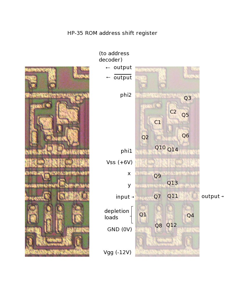
Yes, correctly inferring all the layers from just one image is a problem. I'd prefer not to etch or mechanically delayer the chip if at all possible, and while the unetched images seem like they have a full view of everything for this technology, there are some small areas where ambiguity is possible. The layout is quite idiosyncratic in places, too: isolated areas of metal, gates with no diffusion, etc. Some areas are visibly hacked up to remove design-rule violations. Clearly a hand-drawn design.
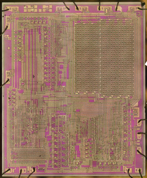
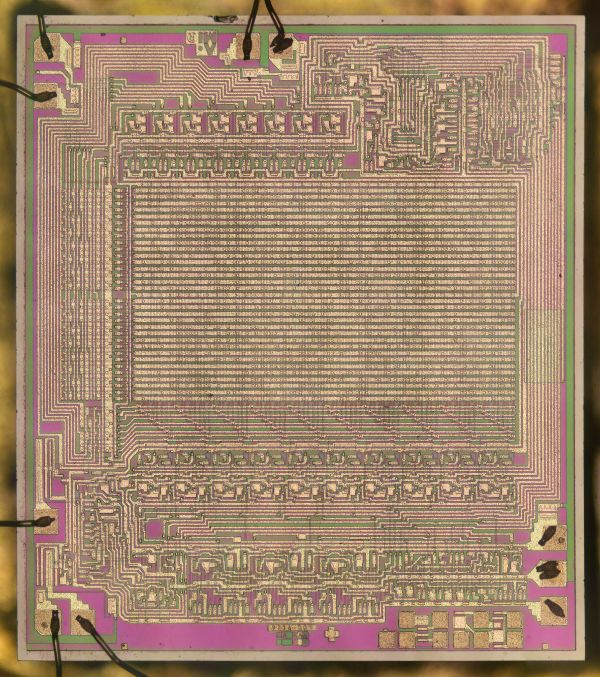
The HP-35 ROM I'm using as a test case is silicon-gate PMOS with depletion loads. You mention identifying depletion implants: I can't see any way to do this for this chip except by context (looking for transistors with gate connected to source). There is no sign of an implant mask under the microscope, even with a 100x high-dry objective I recently got on eBay. Fortunately there are no buried contacts, since there is no poly, but even so it's sometimes tough to distinguish a contact from a gate.
Automatic vectorization is a worthy goal, but the high image quality needed for reliability is beyond my setup, I think, especially with the uncertainty and curve-balls of full custom.
Quote:
Although it's PMOS not NMOS, the circuit style looks comparable.
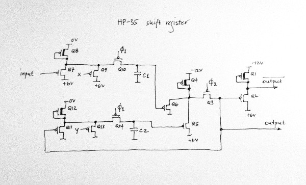
Fortunately the circuit style is conservative: two-phase latches and NOR gates only. (So far.)
Quote:
Let me know if you need any help with the simulator
The visual simulators are cool, but I think I'll stick with verilog for the moment. Since I'm extracting gates and latches I can live with iverilog, but if there were structures that required switch-level simulation I'd have to look at something like IRSIM or another (commercial?) Verilog simulator: iverilog, which is otherwise very good, doesn't support trireg, so the two-phase latches don't work. The latches on this chip are always phi1-inverter-phi2, so I export that whole chunk as a Verilog flip-flop.
I'll certainly keep an eye on visual6502 and the 4004 people---are there any other projects of this general type? It would be nice to have a forum for tools and data; maybe visual6502 will turn into that sort of resource, though last I checked they haven't released their low-level data yet. The existing Web resources on reverse engineering are mostly devoted to failure analysis, understandably enough, and not to recovering and running entire designs of historical interest in totally obsolete IC processes. (Step 3: profit!)
Cheers,
Peter
|