![]() The Museum of HP Calculators
The Museum of HP Calculators
by James H. Fleming and Robert N. Low
ONE OF THE MAJOR advantages of the HP-41C system is its compact size. To achieve high packaging density for each of the instruments of the system at a competitive price, a new hybrid packaging process needed to be developed. The IC package had to satisfy all of the individual product objectives and meet corporate reliability standards.
As an example of the need for the new process, the two 57-pin liquid crystal display driver chips mounted in standard dual in-line packages (DIPs) would occupy about 103 cm , and the space available for the entire display assembly (including LCD and interconnects) was only one-sixth of this volume.
The cost, reliability, and performance (both electrical and environmental) of the new process had to be comparable to or better than a standard plastic DIP. This objective encompassed considerations of manufacturability on a high-volume production line, product flow and yields, testability and reworkability, materials cost and labor, as well as the package's ability to resist environmental stress conditions.
After thoroughly investigating existing technologies, the package configuration shown in Fig. 1 (below) was chosen and implemented. The packaging scheme involves mounting the silicon chip directly onto a high-quality printed circuit board using a conductive epoxy. The IC is passivated in wafer form with a 7000A film of silicon nitride. The chip's inputs and outputs are connected to the printed circuit board using 0.025-mm-diameter gold wires ultrasonically bonded at about 175°C. The IC and wires are encapsulated in epoxy to protect them from mechanical damage or gross condensation. The substrate is then connected to the outside world by a reflow solder operation. The resulting package satisfies all of the design objectives previously mentioned, and is fairly easily implemented, since it employs existing state-of-the-art technologies.

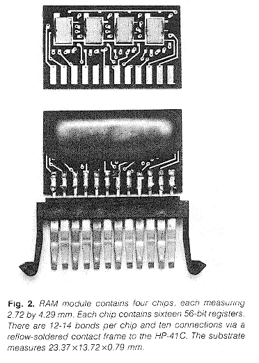
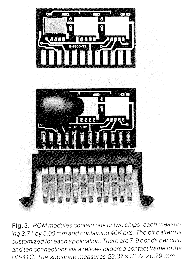
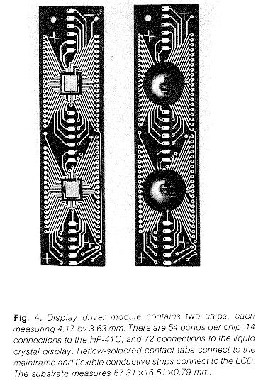
Figs. 2, 3, and 4 are photos of the RAM, ROM, and display driver modules.
The CMOS ICs used in the HP-41C dissipate very little power, and are protected by a silicon nitride passivation layer, so heat dissipation and hermiticity (in the strictest sense) were not problems.
A polyimide/amide, fiberglass-laminate printed circuit board was chosen over a thin-film or thick-film ceramic substrate for reasons of cost, mechanical shock resistance, solderability, and machinability (allows for more diversity in shapes). Polyimide's temperature properties tolerate the high processing temperatures (greater than 175°C) better than standard epoxy/glass printed circuit boards.
State-of-the-art printed circuit board photolithography was required to resolve the 0.13-mm traces and 0.13-mm spaces. Along with the 0.33-mm (#80) plated-through holes, these give the greatest trace density now commercially available on two layers.
The 1/4-ounce copper-clad laminate is plated with a 0.005-mm nickel diffusion barrier and 0.0013 mm of gold to permit reliable bonding of the gold wires.
We would like to extend our sincere appreciation to all those who advised and supported our efforts, especially to Joe Lang, Don Keller, Jim Pollacek, and the entire IC assembly area, to Steve Hall, Sheshadri lyengar and Norm Johnson for the product engineering support in components, to Bob Condor, Les Moore, Tom Pearo, and the rest of the tooling and electronic test group, to the QA department and Hope Keller, whose patience, organization and enthusiasm made qualification possible, and to Thian Nie Khian, Lim Kok Chuan and the rest of the Singapore Division crew for their assistance during the production transfer.
Robert N. Low
Bob Low worked for Hewlett-Packard on the HP-01 during the summer of 1976 while a student at Purdue University, where he received his BS degree in metallurgical engineering in 1977. After graduation from Purdue he joined HP to work on the HP-41C system hybrid development, and then set up the HP-41C production line in Singapore. At present he is working on thin-film printhead evaluation and reliability improvement. Bob is a member of the American Ceramic Society. A native of South Bend, Indiana, he lives in Corvallis, Oregon. Skiing, hiking, carpentry, silversmithing, and sports cars keep his leisure hours busy.
James H. Fleming
Jim Fleming received a pair of BS degrees from Oregon State University, one in production technology (1961) and one in business administration (1962). With HP from 1963 to 1974. he left to form his own product design and manufacturing engineering consulting firm, then returned to HP a year and a half later. He's done product design, production engineering, materials engineering, and manufacturing engineering for several HP divisions and a variety of HP products, the latest being the HP-41C. His consulting work resulted in two patents on biological research equipment. Born in Oakland, California, Jim served in the U.S. Navy, and before joining HP, did mechanical design for a toymaking firm. He and his wife are both licensed pilots and enjoy touring the country in their Cessna 180. They have a son and live in Albany, Oregon. Jim spends his free time on house remodeling, his four-car classic auto collection, and his home-built airplane.
![]() Go back to the HP Journal library
Go back to the HP Journal library
![]() Go back to the main exhibit hall
Go back to the main exhibit hall