![]() The Museum of HP Calculators
The Museum of HP Calculators
by James P. Dickie
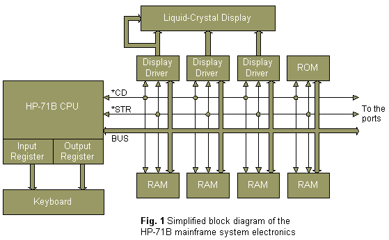
THE ELECTRONICS SYSTEM for the HP-71B Computer is based on seven custom CMOS integrated circuits and a liquid-crystal display (LCD) designed into a package that allows users to customize the HP-71B easily to their needs. A simplified block diagram of the mainframe system is shown in Fig. 1. The system is battery-powered, requiring no power supply, and consists of a CPU and three display drivers mounted on the underside of the keyboard/display printed circuit board. A four-chip 64K-byte ROM hybrid and four 4K-byte RAM hybrids are mounted on the I/O printed circuit board. The four RAM hybrids in combination with the 1.5K bytes of display driver RAM provide 17.5K bytes of built-in RAM. Connections to the four RAM/ROM ports in the front of the HP-71B and the HP-IL (Hewlett-Packard Interface Loop) port in the back of the machine are made via the I/O printed circuit board. The port for the optional card reader connects to the keyboard printed circuit board.
The CPU was designed and optimized for use in handheld computer products. It uses a 64-bit internal word size, operates on a 4-bit data path, and uses 20-bit addresses to provide a 5l2K-byte address space (the largest available in this size of machine). The large address space eliminates the problem previous systems had in bank-switching ROMs and RAMs to obtain a larger memory space. The instruction set is based on the style of architecture used in the HP-41C Computer1 and is oriented toward the arithmetic nature of handheld calculators with the capability of both hexadecimal and binary-coded decimal (BCD) arithmetic.
The CPU incorporates two functions normally delegated to support chips--keyboard control and clock generation. The keyboard logic consists of a general-purpose input register (16 lines) with interrupt capability and a general-purpose output register (12 lines). The output register is also used to drive the daisy chains to each port (see article about memory configuration) and, in combination with external circuitry, to drive the piezoelectric beeper at one of two selected audio levels.
Three display driver ICs drive the 8-row-by-136-column (including annunciators) liquid-crystal display. One of these three drivers acts as the master and generates the display clock, the voltage reference, and the display-on signal used by the other two display chips (slaves). A 4-bit software-controlled register modifies the display contrast and optimum viewing angle by adjusting the value of the voltage reference signal. The master/slave function and addressing of a display driver chip are selected by two configuration pins that are tied high or low on the printed circuit board. Each driver chip supplies 512 bytes of hard-configured RAM and a 24-bit crystal-controlled oscillator timer with 1/512-second resolution. The timers are used by the HP-71B's operating system to implement the real-time clock system.
The optional 82400A Card Reader Module provides the HP-71B Computer with inexpensive mass storage. The handpulled magnetic cards can each record up to 1300 bytes. The card format and modified frequency modulation (MFM) coding are the same as that used by the internal card reader of the HP-75 Computer,2 which allows an interchange of TEXT files recorded with the HP-75's LIF1 format.
The 82400A consists of a two-chip hybrid, the external components for the analog circuit, and a three-coil magnetic head in a self-aligning mount. The analog IC, which is a modification of the IC2,3 used by the HP-75's card reader, receives signals from the head and converts them to digital signals. The hybrid digital IC converts the serial MFM coding into data bytes and buffers them for the HP-71B.
The 82401A HP-IL Interface Module (see box) provides the HP-71B with high-speed I/O and the capability to drive the whole line of HP-IL peripherals. This module is the first HP-IL interface that supports the entire HP-IL definition in the base configuration. Using primary addressing, up to 31 peripherals can be controlled, and up to 930 peripherals can be controlled through secondary addressing. The 82401A is designed to allow the HP-71B to be a loop device or controller as well as an interface for up to three loops.
The 82401A consists of a two-chip hybrid containing a 16K-byte ROM and a newly designed I/O processor that allows block communication transfer rates in excess of 5000 bytes/s. Also included are discrete components required for isolation, electrostatic discharge (ESD) protection, and impedance matching.
The HP-71B bus structure was developed for use in handheld computer products. The structure maximizes the performance of the system while minimizing the interconnect required for each system IC or port.
The system bus is a fully multiplexed 4-bit address, instruction, data, and command bus. In addition, there are two control signals--a bus clock *STR (also referred to as strobe) and a command/data signal *CD. The bus commands used by this system are listed in Table 1 (below). *STR is driven by the CPU and serves to synchronize all bus transfers. *STR is not a true system clock, since it can remain inactive (high) for cycles when the CPU is busy performing internal operations. The *CD line indicates whether data on the bus is a command (*CD low) or data (*CD high). In addition, memory devices may have two other lines: DAISY-IN and DAISY-OUT. The architecture of this system allows memory to be located dynamically in the overall address space of the CPU (512K bytes) and these two lines are used during the address assignment process (soft configuration, see article).
All bus operations are initiated by the CPU. The CPU starts a specific transfer on the bus by driving the *CD line low before *STR goes low. While *CD and *STR are low, the CPU drives a command on the bus and all devices in the system latch the command on the rising edge of *STR This strobe is referred to as a command strobe. The command issued during a command strobe specifies the operation that is to be performed on each succeeding *STR until another command is issued. At all times when data or an address is being transferred, *CD is held high. A strobe issued while *CD is high is referred to as a data strobe.
| Code | Mnemonic | Action |
|---|---|---|
| 0 | NOP | All devices ignore STR until a new command is loaded. |
| 1 | ID | The unconfigured device that sees its daisy-chain input high sends its five-nibble identification code on the following data strobes. |
| 2 | PC READ | Read using program counter. The device selected by the system program counter sends data addressed by its local program counter on the following data strobes. All devices increment their local program counters each data strobe. |
| 3 | DP READ | Read using data pointer. The device selected by the system data pointer sends data addressed by its local data pointer on the following data strobes. All devices increment their local data pointers each data strobe. |
| 4 | PC WRITE | Write using program counter. The device selected by the system program counter loads the data on the following strobes into the location addressed by its local program counter. All devices increment their local program counter each data strobe. |
| 5 | DP WRITE | Write using data pointer. The device selected by the system data pointer loads the data on the following data strobes into the location addressed by its local data pointer. All devices increment their local data pointer each data strobe. |
| 6 | LOAD PC | Load program counter. All devices load the data on the following data strobes into their local program counter, low-order nibble first. After all five nibbles are transferred, the command code is automatically changed to 2. |
| 7 | LOAD DP | Load data pointer. All devices load the data on the following data strobes into their local data pointers, low-order nibble first. After all five nibbles are transferred, the command code is automatically changed to 2. |
| 8 | CONFIG | The unconfigured device that sees its daisy-chain input high loads the following five data nibbles into its configuration register, low-order nibble first |
| 9 | UNCNFG | The device currently addressed by its local data pointer unconfigures itself. The device then responds to CONFIG and ID commands only. The local data pointers must be loaded immediately preceding an UNCNFG command. |
| A | POLL | All chips that require service pull one data line high during the next STR low |
| B | Reserved. | |
| C | BUSCC | The device currently addressed by its local data pointer performs a specialized operation as defined by the individual device. |
| D | Reserved. | |
| E | SHUTDOWN | When the CPU has received a SHUTDN instruction it issues this command and turns off its oscillator. Each device responds based on its own special requirements. |
| F | RESET | All devices reset their configuration flags (if applicable) and perform other local resets based on their own special requirements. |
Each device that resides on the HP-71B system bus has two 20-bit address registers--the local program counter and the local data pointer. A device responds to data reads and writes only if its local address register (program counter or data pointer depending on the read or write command) is within its address configuration. Only the address of the first nibble of data to be transferred needs to be sent, since both the program counter and the data pointer are capable of incrementing once each data strobe. This greatly reduces the movement of addresses on the bus. Each device is either permanently addressed (hard-configured) at a specific address or capable of being dynamically located (soft-configured) at many addresses.
A soft-configurable device also has an ID register and a configuration register. The ID register is a 20-bit read-only register programmed to provide device specific information required to identify its classification (RAM, ROM, memory-mapped I/O, etc), memory size, and in some cases, positional information (such as last device in a module). The configuration register is up to 20 bits in length and positions the device within the system memory space. The actual size of this register is determined by the number of upper-order bits required to specify the device completely.
The HP-71B's operating system allows soft-configured devices to have address spaces ranging in size from 8 bytes to 128K bytes. All devices are configured such that the upper-order bits of the local address register are compared with the upper-order bits of the device configuration register (hard or soft). If these bits are identical, the device has an address match and responds to read and write commands. The number of upper-order bits compared is determined by the number required to specify the device's memory size within the total address space. For example, a device with an address space size of 1K bytes (2K nibbles) requires eleven bits of address, leaving the upper nine bits for its configuration address.
A soft-configured device powers up unconfigured. When unconfigured, a device only responds to the ID and CONFIG commands and drives its DAISY-OUT line low. The ID command identifies a device before it is configured in the system. If a soft-configured device is unconfigured and sees its DAISY-IN line high, it outputs its five-nibble identification code (low-order nibble first) on the five data strobes that follow the ID command.
A soft-configured device is assigned its configuration address by the CONFIG command. If an unconfigured device sees its DAISY-IN line high, it loads the configuration address issued on the five data strobes immediately following the CONFIG command (low-order nibble first) into its configuration register. A device may latch only the number of high-order bits it requires as determined by its memory size. On the following command strobe, the device sets its configuration flag.
Once configured, a device no longer responds to either an ID or a CONFIG command, and drives its DAISY-OUT line to the same logic level as its DAISY-IN line. The DAISY-OUT line of one device may be tied to the DAISY-IN line of a second device. In this manner many devices are daisy-chained together so that they are configured individually to different addresses. After being configured, a device waits until the next command strobe to set its configuration flag. This delays the change in its DAISY-OUT line so that the next device on the daisy chain is not configured simultaneously.
A device may be unconfigured by either a RESET or an UNCNFG command. The RESET command simultaneously unconfigures all soft-configured devices in the system. A device responds to an UNCNFG command by clearing its configuration flag if the data pointer is within its address configuration.
A hard-configured device powers up configured to a specific address and does not respond to an ID, CONFIG, or UNCNFG command. A RESET command does not affect its configuration. If the device has a DAISY-OUT line, it is always driven to the same logic level as its DAISY-IN line.
The CPU reads the contents of a specific address location by first sending a LOAD PC or LOAD DP command followed by the five-nibble address. The address is sent, least-significant nibble first, with the data being latched on the rising edge of *STR. After the last address nibble is loaded, the command automatically changes to a PC READ or DP READ and the addressed device sends one nibble each strobe. The CPU may also perform a read without sending a new address by issuing a PC READ or DP READ command. The addressed device responds by sending one nibble each strobe.
The CPU writes the contents of a specific addressed location in a similar manner. The address need not be loaded before a write operation. A write is performed by issuing a PC WRITE or DP WRITE command followed by the data to be written. If the address is required before the write operation, the CPU issues a LOAD PC or LOAD DP command followed by the five-nibble address. After the address is loaded, the CPU issues a PC WRITE or DP WRITE command and places the data to be written on the bus.
All devices increment their local address registers once each data strobe during read and write operations. It is possible for a read or write operation to begin in one device and cross the address boundary into another device. Currently the CPU reads or writes up to 16 nibbles during an operation, but the architecture allows reading and writing more than 16 nibbles at a time.
The CPU has two fundamental states--operating and standby. To place the CPU in standby mode, a SHUTDN instruction is issued. The CPU sends the SHUTDOWN command and on the ensuing cycle stops the system clock (*STR) and its own clock. In standby mode, all CPU-resident and system memory is preserved.
The CPU is brought out of standby mode either by pulling an input register line high (pressing a key), or by driving the *CD line low. On wakeup the CPU starts its clock and immediately drives *CD low with a NOP command. If the CPU detects that a severe low-voltage condition has occurred while it was in standby mode, the CPU program counter is forced to zero and hexadecimal mode arithmetic is asserted. A LOAD PC is the first command issued after the NOP command and the current CPU program counter value is loaded into all devices' local program counters. At this point, the standard instruction fetch sequence is initiated. If the CPU was awakened by an input register and interrupts are enabled, then a normal interrupt occurs before an instruction fetch.
*CD is driven low to wake up the CPU by a device in the system that needs service while the system is in standby mode. If a device wakes up the CPU and the CPU shuts down without satisfying the device's need for service, the device may not wake up the CPU again until the service request has been satisfied. This avoids a situation where the operating system does not know how to handle a device's service request and therefore is not allowed to shut down.
If a device needs service while the CPU is operating, it must either wait until the CPU executes a service request instruction (SREQ), or if it has the capability, interrupt the CPU using IR14 (available at all ports). The SREQ instruction causes the CPU to issue a POLL command, followed by one data strobe during which the CPU latches the bus data in the manner of a usual read. A device may respond to the service poll by pulling one of the bus lines high. Since the CPU precharges the bus low every cycle before *STR goes low, the data read by the CPU is a binary OR of all device responses.
The following HP-71B devices can wake up the CPU and can respond to a service poll on the bus line shown:
| Device | Bus Line | Service Request |
|---|---|---|
| Display Driver | Bus[0] | Timer underflow |
| HP-IL Chip | Bus[1] | Data available, interrupt, power-on reset, loop service request |
| Card Reader | Bus[2] | FIFO (first in, first out) servicing, error condition. |
There were many engineers who made significant contributions to the development of the electronics for the HP-71B. Among these, Dave Rabinowitz made valuable contributions to the bus architecture and CPU definition, Dan Rudolph designed the display driver IC, C. T. Wang designed the RAM IC, Van Walther designed the ROM, John McVey characterized the CPU and pushed it into production, Bob Puckette became our ESD/EMI expert, and Carl Johnson provided overall system support. The HP 82400A Card Reader Module was developed by Megha Shyam, Bill Saltzstein, and Loren Heisey. A family of I/O processors that include the processor for the 82401A HP-IL Interface Module was developed by Dave Rabinowitz, Grant Garner, Don Reid, Dave Serisky, Preston Brown, and Charles Brown.
A special thanks to the many people in HP's Corvallis Components Operation who made significant contributions to the support of the ICs designed. These include Max Schuller, Tim Hubley, Bob Dunlap, Mike Gilsdorf, Dane Rogers, Stan Gibbs, Scott Linn, Jim Hutchins, Joe Szuecs, Von Soutavong, Doug Peck, Gary McDaniel, and the rest of the packaging and fate personnel who made major efforts to help the project succeed.
References
1. B.E. Musch, J.J. Wong, and D.R. Conklin, "Powerful Personal Calculator System Sets New Standards," Hewlett-Packard Journal, Vol. 31, no. 3, March 1980.
2. K.R. Hoecker, et al, "Handpulled Magnetic Card, Mass Storage System for a Portable Computer,'' Hewlett-Packard Journal, Vol. 34, no. 6, June 1983.
3. T.J. Arnold and B.E. Thayer, "Integration of the HP-75's Handpulled Card Reader Electronics in CMOS," ibid.
![]() Go back to the HP Journal library
Go back to the HP Journal library
![]() Go back to the main exhibit hall
Go back to the main exhibit hall