HP Articles Forum
[Return to the Index ]
[ Previous | Next ]
HP-49G+ -- A Look Inside . . .
Posted by Paul Brogger on 8 Dec 2003, 9:50 p.m.
I was able to get my HP-49G+ apart and take a few pictures. I thought I'd share them with you all, and Dave has been kind enough to host them for us.
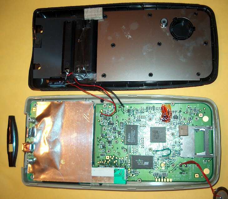
The first one shows the two halves not quite fully separated, and the IR lens removed.
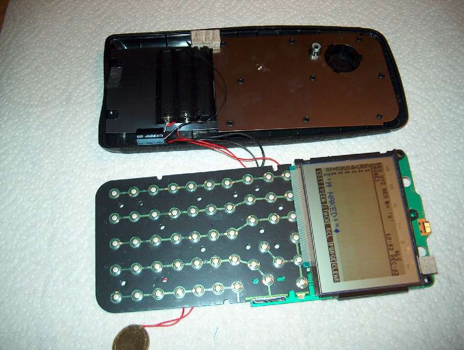
The upper, dark section is the inside of the bottom case half. The battery compartment is to the left, and the wires connect the AAA and backup batteries and a large electrolytic capacitor to the main board. The small silvery rectangle near the top is a piece of conductive foam serving as the negative battery contact with the PCB. The larger black circle is where the buzzer is mounted, the smaller concentric circles to its upper left are the reset switch (a springy rubber contact).
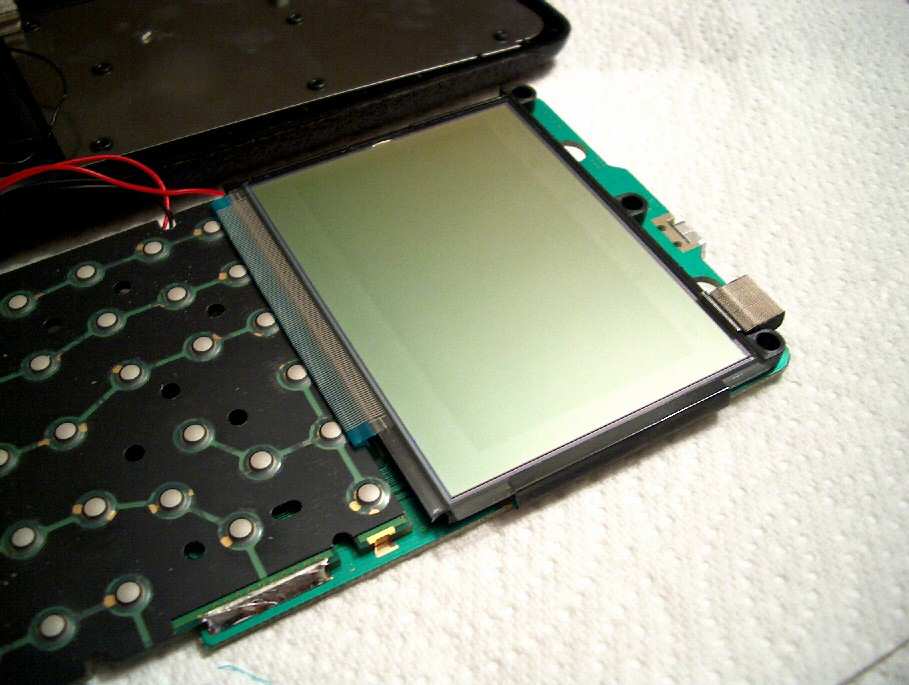
The lower half shows the front case half, with the LCD board on the left covered by self-stick foil-backed paper. (It's actually aluminum-colored -- it looks coppery in these pictures, for some reason.) The main (CPU/key/SD) board is on the right.
The IR lens is thin and flexible, and pops out easily, but would probably be hard to get back in without taking apart the case halves (at least partially).
The second picture shows the electronics a bit more closely. A capacitor is glued to the main board with a smear of red-orange goo, and the reset contact is some gold fingers interleaved near the blue jumper wire.
The main board connects to the LCD board via: 1) a mylar (?) ribbon that runs across the calculator, just to the right of the coppery-looking shielding, and 2) a series of solder connections along two edges of what looks like a rectangular extension of the LCD board, near the bottom of the picture.
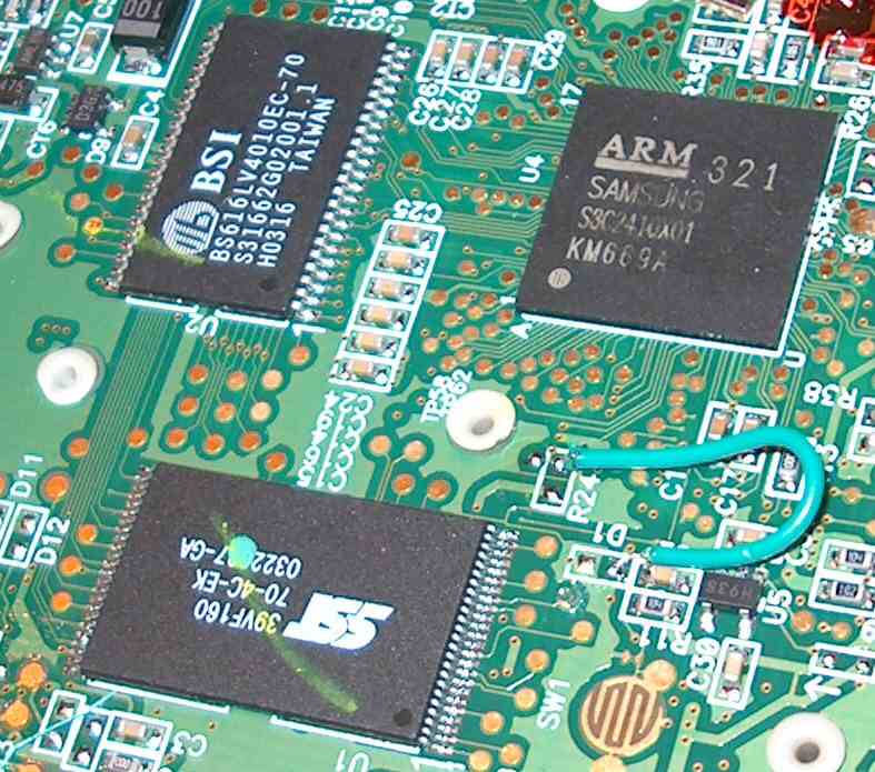
The square black chip above & to the right is marked "ARM" -- the other two I haven't looked at too closely. There's another pad of conductive foam attached to the SD card slot assembly.
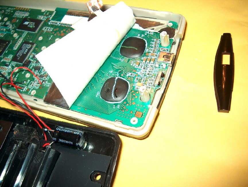
The third image shows most of the self-stick paper/foil backing peeled away from the LCD board, exposing two blobs of black stuff apparently sealing LCD controller chips on the board.
Also visible are the IR sender & receiver, and the USB mini-B socket.
This view gives a good idea how the thing is put together -- the two posts are what I drilled to free up the top end, and otherwise it's only a series of plastic tabs around the edge that lock into the bottom case. After "topping" the posts, the two halves snapped apart quite easily.
BTW, the black accent that surrounds the calculator face is actually applied, and the calculator’s gold-colored front and "side bumper" are actually one piece. Don't pry upward on the black accent, as it's just decoration and won't get you anywhere.
And, in case you're wondering, this unit is not dead -- it survived the "operation" fine. One key is that I didn't try to pull the self-stick aluminized paper completely off, as it's in contact with the LCD edge of the mylar ribbon connecting the two circuit boards. I think that, were I to try to take all of the sticky paper/shielding off, the ribbon connector may well come with it
Addendum: More Images
49G+ Chips Close-up
In response to a request, I took and posted a close-up of the chips, and someone chimed in with an explanation.
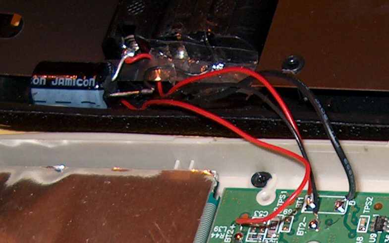
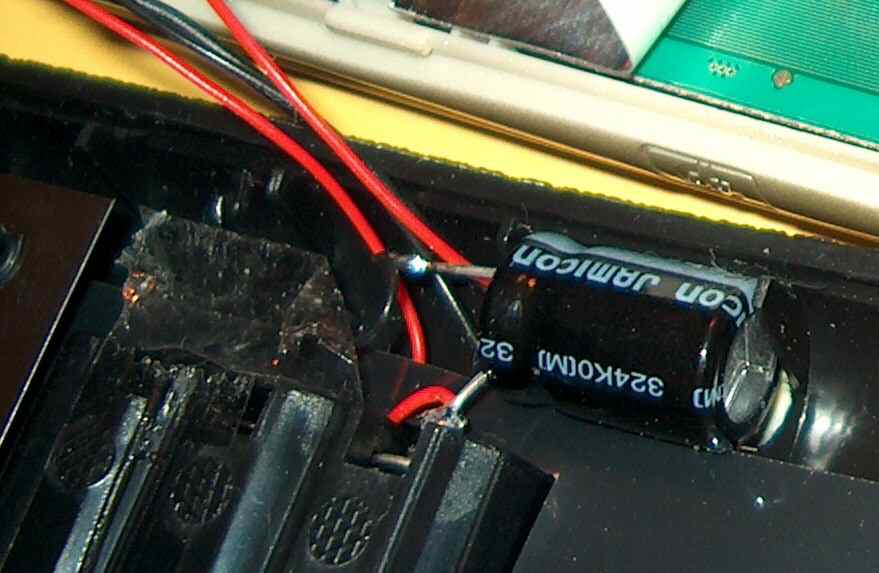
49G+ Battery Compartment Close-ups
In response to a thread in comp.sys.hp48 about concern over stretching springs in the battery compartment to fix battery contact problems, I took several close-ups of the compartment from the inside.
The first three were taken with the cellophane tape and plastic insulating sheet in place:
1. battery compartment close-up 1
The fourth was taken with the cellophane tape removed to expose the wires more clearly:
4. battery compartment close-up 4
The last was taken with the black plastic insulator/shield sheet folded toward the camera, to expose the back-up battery and its connections:
5. battery compartment close-up 5
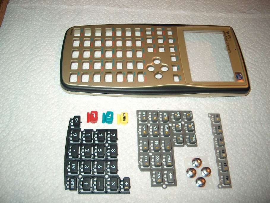
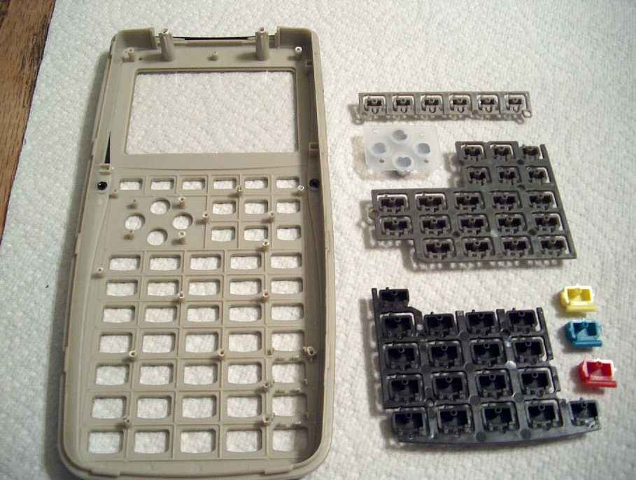
49G+ Keyboard Close-ups
Perhaps the most talked-about issue surrounding the introduction of the 49G+ has been early problems with its keyboard. I felt that the disassembly would not be complete without a close look at how its keyboard was actually put together:
1. PCB removal