The Museum of HP Calculators

HP Forum Archive 14

[ Return to Index | Top of Index ]

What are these pads for on the HP49G+ circuit board?
Message #1 Posted by Bruce Horrocks on 16 Dec 2003, 7:12 p.m.

Something is puzzling me regarding the picture of the HP49G+ circuit board that Paul Brigger took and posted here at URL <http://www.hpmuseum.org/guest/brogger/hp49gpi1.jpg>. (Each of these pictures is marvellous, by the way.)

Regarding the one in question though, look at the left side of the main circuit board (from the calculator's point of view, the bottom of the picture according to the picture's orientation.) I count six pads on the very edge of the circuit board which look as though something should connect to them but there doesn't appear to be anything in the case that makes contact with them.

Appearances can be deceptive though: perhaps Paul has another photograph that shows the matching side of the top cover so we can see if anything marries up to them?

Let the speculation begin...

:-)

      
Re: What are these pads for on the HP49G+ circuit board?
Message #2 Posted by Joerg Woerner on 17 Dec 2003, 2:26 a.m.,
in response to message #1 by Bruce Horrocks

Looks like a connection to programm the Flash memory or debug the ARM software. Regards, Joerg

      
Re: What are these pads for on the HP49G+ circuit board?
Message #3 Posted by James M. Prange on 17 Dec 2003, 6:10 a.m.,
in response to message #1 by Bruce Horrocks

Has anyone taken a 48gII apart? If so, is the PCB similar to the 49g+'s? And if it is, where does the 48gII's serial I/O connect to the PCB?

Wouldn't it be great if the RS-232 type serial I/O were accessible on the 49g+ and it were just a matter of connecting it?

After all, I've read that the 48gII and 49g+ use the "same" ROM, although I don't know whether that's entirely true.

I assume that one would have to refrain from connecting both the USB and an RS-232 serial type device at the same time.

Regards,
James

            
HP49G+ LCD lines
Message #4 Posted by Vieira, Luiz C. (Brazil) on 18 Dec 2003, 12:51 a.m.,
in response to message #3 by James M. Prange

Hi;

I noticed that tha HP49G+ has a different, 2-lines +, LCD. Unless their ROM is based on selectable parameters for each model (graphics, objects to be shown, etc.), I understand that some differences should be taken into account when LCD data "building" is considered.

Or not?

My 2¢.

Luiz (Brazil)

      
Re: What are these pads for on the HP49G+ circuit board?
Message #5 Posted by Paul Brogger on 17 Dec 2003, 9:37 a.m.,
in response to message #1 by Bruce Horrocks

The picture you cite is the second of the several images taken. The first <http://www.hpmuseum.org/guest/brogger/hp49gpi0.jpg> shows the back and front halves, separated, but complete.

There is nothing in the calculator that mates to those pads. I noticed them upon opening the calculator, and have assumed they are contacts used for Q.C. tests during manufacture.

            
Re: What are these pads for on the HP49G+ circuit board?
Message #6 Posted by Nelson M. Sicuro (Brazil) on 17 Dec 2003, 10:09 a.m.,
in response to message #5 by Paul Brogger

Maybe these contacts are for JTAG programming/testing, just complementing what you said.

Best regards,

Nelson

                  
Re: "JTAG" & "Boundary Scan" Definitions
Message #7 Posted by Paul Brogger on 19 Dec 2003, 12:23 p.m.,
in response to message #6 by Nelson M. Sicuro (Brazil)

FYI, I thought I'd share an interesting tutorial I found about JTAG and "Boundary Scanning": < http://www.ezytech.com/asset/pdfs/boundaryscan_tutorial.pdf >.

Ya lern sumpin evry day!

                  
Re: What are these pads for on the HP49G+ circuit board?
Message #8 Posted by Veli-Pekka Nousiainen on 20 Dec 2003, 6:57 a.m.,
in response to message #6 by Nelson M. Sicuro (Brazil)

"Maybe these contacts are for JTAG programming/testing, just complementing what you said."

I finally opened my 49g+ and yes it is a JATG interface on the edge. I've seen that thing before. Maybe I will drill my case to open it from that point?

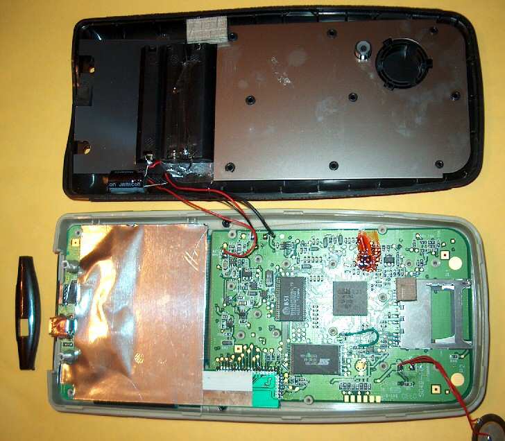
Opening: Above the backup battery are two white soft plastic rivets. I dug them out using a dull knife and pulled the top a little and then using a pensil as a lifter pulled the IR protector out with the knife. Next I used the knife to go carefully around the calculator removing the black frame. Then I just pulled from top (watching for the tension to the plastic) and the case started to snap open. There are two thin plastic rivets maybe on the cursor approximity that will brake during the operation. Shake them out and glue them into your collectors book (you have one/many - don't you?).

To take a good look inside you also need to loosen the piezo buzzer by gently pulling the tape covering the wires away from the case half.

Assembly is a snap. Do evrything in reverse order. The IR cover is thou good to put in before closing the cases.

Naturally you know how to ground yourself while handling CMOS circuitry!

[VPN]


[ Return to Index | Top of Index ]

Go back to the main exhibit hall